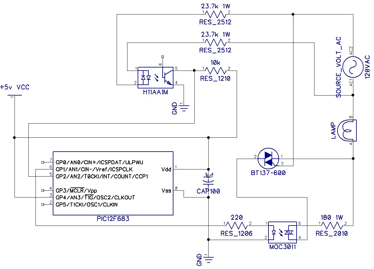
Sorry this took longer than expected. Hopefully I did not make any mistakes creating the schematic after the fact but I am pretty sure I did not. I'm using diptrace to produce the schematic and I've only used it a few times. Here is the picture of my schematic and code. This is working really good I've had it on for several days and have not seen anything going wrong however I am open to suggestions/criticism if anyone spots anything and wants to comment please feel free.
Regards
David
Code:
    ' LightHouse Lamp dimmer
    ' ======================
    '
    ' File name : Lighthousemorse.pbp
    ' Programmer : David C. Bittner
    ' Date : 2020-07-02
    ' Device : PIC12F683
    '
    ' This program is use to dim intensity of an AC line load
    ' like lamp, motor and other.  Developped for 60 Hz line.
         '
    ' The software need :
    '     1. A full wave signal from the AC line on GP2/INT
    '
TRISIO = %00101101        ' All input except GP1 GP4  GP1 out to TRIAC
OPTION_REG.7=0            ' Enable pull-ups
OPTION_REG.6=1            ' Interupt on rise
CMCON0 = 7                ' Disable analog comparator
ANSEL=0                   ' Disable analog converter
Triac  var GPIO.1 ' Output to TRIAC gate
ACLine var GPIO.2 ' Input for the FullWave rectify AC line
morse  var GPIO.5 ' used to check switch if 1 operate as dimmer, 0=morse out
outp   var GPIO.4
    '
    '        Variable definitions
    '        ===================+
    '
TriacDelay var Word
counter var word
timercount var word
updown var bit
unit var word
counter=0
unit = 500

TRIAC=1  'TEST TO MAKE SURE LIGHT COMES ON
PAUSE 1000  'LEAVE IT ON FOR 1 SECONDS
triac=0
pause 5000   ' wait 5 seconds before starting
triacdelay=8000
ON INTERRUPT GOTO ACDetect
INTCON=%10010000 ' Enable interrupt on GP2/INT change

updown=1       '1=dim to bright, 0=bright to dim
start:
   '
   ' do what we need to in this routine if more
   '
   if morse=1 then
      triac=1
      outp=1
   else
      outp=0
      triac=0
      gosub morsecode
   endif
goto start
morsecode:
     pause 2000
     triac=1     ' W
     pause 400   'dot
     triac=0

     pause 400
     triac=1
     pause 850   'dash
     triac=0

     pause 400
     triac=1
     pause 850   'dash
     triac=0

     pause 800
     triac=1     'E
     pause 400   'dot
     triac=0

return    '
    '       ACDetect
    '       --------
    '
    ' Interrupt routine called by ACLine (GP2/INT) pin state change
    '
disable
ACDetect:
    'pauseus 240
    counter=counter+1
    if counter==5 then
        counter=0
        if updown==1 then
            triacdelay=triacdelay-100
            if triacdelay==-100 then
                'triacdelay=8000
                updown=0
            endif
        endif
        if updown==0 then
            triacdelay=triacdelay+100
            if triacdelay==8100 then
                updown=1
            endif
        endif
    endif
    triac=0
    pauseus triacdelay
INTCON.1=0
resume
enable
Attachment 8898


 to conduct both ways (AC).


Bookmarks