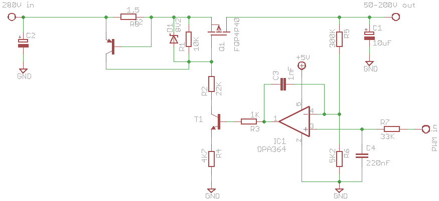
It was late when I replayed and didn't look in to schematic too much. And now it late again, so sorry in advanced if I miss something.
You are right, for P channel configuration is correct. Your design look like LDO. And that is inherently unstable. So watch out for that.
Left schematic for NPN will not work as expected. Collector base is reverse biased. And it act as diode.
So that is reason mosfet is cut of. Voltage drop across diode is much lower than Vgs threshold.
NPN current limit is tricky to implement here, because collector must be on higher potential than base...
PNP circuit should work. Or to be precise must work. I suspect that pin out is wrong or you didn't use PNP transistor. If pin out is wrong, T2 isn't correctly biased. I would start with transistor tester, or create simple circuit with PNP just to be sure is it what you think it is and pin out is correct. Try to disconnect base and see is it working. Measure voltage across 1.5R R8(current sense resistor, I don't see clearly part name) with and without base connected.
Also just to remind you that you are measuring output current and current thru R1. So take that in account. With 22K current is 12mA, so across R8 is only 20mV, not enough to bias BE junction, but check voltages current and resistor values. I'll also suggest that you move high side od R1 to 280Vin so it wont affect current limiting.
Bookmarks