New version of Darrel Taylor's Elapsed include for 64MHz:
Code:
'***************************************************************************
'*  Name    : Elapsed_INT-18.bas                                           *
'*  Author  : Darrel Taylor                                                *
'*  Date    : JUL 11, 2006 : 7/11/2010 : Dec 23, 2014                      *
'*  Version : 1.3                                                          *
'*  Notes   : Must have DT_INTS-18.bas loaded first                        *
'*   ver 1.2: Now works at any OSC frequency without using the prescaler   *
'*   ver 1.3: will work with 64MHz thanks to Sheldon                       *
'*            New field ONEHUNDRETH is now used instead of TICKS           *
'***************************************************************************
DISABLE DEBUG

; syntax =     Handler  IntSource,        Label, Type, ResetFlag?
DEFINE  Elapsed_Handler  TMR1_INT,  _ClockCount,  asm,  yes
; the above define can be used in the INT_LIST macro, if desired (optional)

Ticks            VAR BYTE   ; Counts timer Overflows
OneHundreth      VAR BYTE    ; New field for 64MHz
;T1Post           VAR BYTE   ; Timer1 postscaler
Seconds          VAR BYTE
Minutes          VAR BYTE
Hours            VAR BYTE
Days             VAR WORD

OneHundrethChanged     VAR BIT    ; New field for 64MHz
SecondsChanged   VAR BIT    ; idicates that the value has changed
MinutesChanged   VAR BIT
HoursChanged     VAR BIT
DaysChanged      VAR BIT

GOSUB ResetTime             ; initialize the Elapsed Timer

Goto OverElapsed            ; skip over the routines

' -------------- calc timer reload Constants -------------------------------
ASM
T1PS = 1                             ; start with 1:1 postscaler
TimerConst = ((OSC*1000000)/4/100)   ; how many timer ticks will it take
  while TimerConst > 65400           ; if it's more than the timer can count
T1PS = T1PS * 2                      ;   double the postscaler
TimerConst = TimerConst / 2          ;   halve the count
  endw
TimerConst = 65536 - TimerConst + 8  ; final reload value


; -----------------  ADD TimerConst to TMR1H:TMR1L -------------------------
ADD2_TIMER   macro
    BCF     T1CON,TMR1ON, 0       ;  1 Turn off timer
    MOVLW   LOW(TimerConst)       ;  1
    ADDWF   TMR1L,F, 0            ;  1
    BTFSC   STATUS,C              ;  1/2
    INCF    TMR1H,F, 0            ;  1
    MOVLW   HIGH(TimerConst)      ;  1
    ADDWF   TMR1H,F, 0            ;  1
    endm

; -----------------  ADD TimerConst to TMR1H:TMR1L and restart TIMER1 ------
RELOAD_TIMER  macro
    ADD2_TIMER
    BSF     T1CON,TMR1ON, 0       ;  1   Turn TIMER1 back on  (8 cycles)
    endm

; -----------------  Load TimerConst into TMR1H:TMR1L ----------------------
LOAD_TIMER  macro
    MOVE?CT  0, T1CON,TMR1ON
    MOVE?CB  0, TMR1L
    MOVE?CB  0, TMR1H
    ADD2_TIMER
    endm
ENDASM

' ------[ This is the Interrupt Handler ]-----------------------------------
T1PS  CON EXT
ClockCount:
@ RELOAD_TIMER                   ; Reload TIMER1
Ticks = Ticks  + 1                      ; each tick is 2.5ms
'       IF LATD.3 = 0 THEN                  ' used to debug to confirm 2.5ms
'          LATD.3 = 1
'       ELSE
'          LATD.3 = 0
'       ENDIF
  if ticks // T1PS = 0  THEN      ' if modulas of tips (4) = 0
'       IF LATD.3 = 0 THEN                  ' used to debug to confirm 10ms
'          LATD.3 = 1
'       ELSE
'          LATD.3 = 0
'       ENDIF
          OneHundreth = OneHundreth + 1   ; each 1/100th is 10ms
          OneHundrethChanged = 1
          IF OneHundreth  = 100 THEN
              OneHundreth = 0
'    Ticks = Ticks + 1
'    IF Ticks = 100 THEN
'       Ticks = 0
'       T1Post = T1Post + 1
'       IF T1Post = T1PS THEN
'           T1Post = 0
           Seconds = Seconds + 1
           SecondsChanged = 1
           IF Seconds = 60 THEN
              Seconds = 0
              Minutes = Minutes + 1
              MinutesChanged = 1
           ENDIF
           IF Minutes = 60 THEN
              Minutes = 0
              Hours = Hours + 1
              HoursChanged = 1
           ENDIF
           IF Hours = 24 THEN
              Days = Days + 1
              DaysChanged = 1
              Hours = 0
           ENDIF
       ENDIF
    ENDIF
@ INT_RETURN                     ; Restore context and return from interrupt

'-----====[ END OF TMR1 Interrupt Handler ]====-----------------------------

StartTimer:
    T1CON = 1                    ; 1:1, FOSC4, TMR1ON
RETURN

; --------------------------------------------------------------------------
StopTimer:
    T1CON.0 = 0                  ; Turn OFF Timer1
RETURN

; --------------------------------------------------------------------------
BitSave  VAR  BIT

ResetTime:
    BitSave = T1CON.0            ; Save TMR1ON bit
@   LOAD_TIMER                   ; Load TimerConst
    T1CON.0 = BitSave            ; Restore TMR1ON bit
;    T1Post = 0                   ; clear the postscaler
    Ticks = 0
    OneHundreth = 0
    Seconds = 0
    Minutes = 0
    Hours = 0
    Days = 0
    OneHundrethChanged = 1
    SecondsChanged = 1           ; indicate everything has changed
    MinutesChanged = 1           ; so that 00:00:00 is processed
    HoursChanged = 1
    DaysChanged = 1
RETURN


OverElapsed:
ENABLE DEBUG
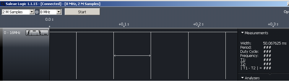
New field OneHundreth (10ms) replaces Tick (2.5ms at 64MHz).
(Remove .TXT suffix)
Elapsed_INT-18_64MHz.bas.txt
Robert


Bookmarks