


Well... In the "old days" I used to build projects with through-hole parts on "vectorboard" (or perfboard, or punchboard, or whatever other names it goes by).
That worked for me for prototyping projects for about 30 years.
And if I made a mistake I could unsolder something and "move it over there" and re-solder it...
Then one day I woke up to find that a lot of the "cool" new parts that I'd like to use are only available in surface mount packages. Sigh.
So I finally set myself up with enough equipment to do SMD's and I started laying out (and paying for ) boards for most of my projects. But small runs of boards are EXPENSIVE, so I've gotten pretty good at maximizing my board usage to get the most parts on the least amount of real estate. I've done quite a few pretty dense 2-layer boards with good success. (Don't ask about the RTC that got laid out "upside down" on one board... I felt really stupid with a magnifying glass and tweezers bending the leads on the IC's to point upwards so I could mount it upside down on the board. )
Anyway, now I've got a new project that needs to fit in a very tight space.
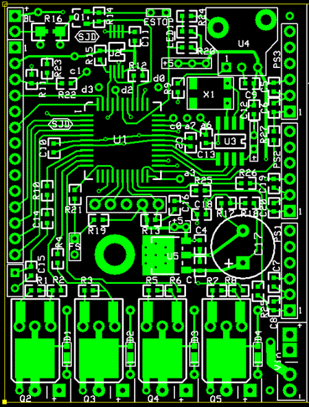
I've got 6 IC's including 16F887, an RTC and xtal, EEPROM, voltage regulator, digital pot, and IR detector. (mostly TQFN, TSSOP, and DPAK packages)
There's also 5 MOSFETS, 4 in DPAK and 1 in SOT223.
And there's a few diodes, a crystal, a 470uF electrolytic cap (big!), and a metric ****load of resistors and caps, mostly in 0603 packages.
All together there's 59 parts that live ON the board, plus connectors to connect a 2x16 LCD, several external sensing devices, and power and programming connectors.
The problem? It's all gotta fit on less than *5*square inches of real estate. I've got about 2" x 2.5" of space to work with.
I've banged my head against it for days now trying to make it fit on a 2 layer board, but I just can't quite get there. I'm using the smallest packages available (or that I can work with) but it just ain't gonna go on 2 layers in the space I've got to work with.
If I go to a 4 layer board it should work . It's tight... but it'll fit.
SO... Are there any special tips I should know about for laying out 4 layer boards? I've done plenty of 2 layer, and in theory 4 layer should be easier... But 4 layer is so much more expensive and I don't want to do something obviously stupid and wreck it.
I've got power and ground on the inner layers and all my signal stuff on the outers. Everything *looks* like it's OK, but I think I've got the fear in me because it's my first time.:
Any words of wisdom before I jump into the world of 4-layer and blow $120 for 6 boards that are only 5 square inches each?
steve


 and I don't relish the idea of soldering one side by hand. I know there's special glues available for that, but that takes more time so I'd rather not populate both sides if I can avoid it.
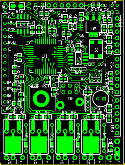


Bookmarks