Thanks Guys for all the good suggestions!
If this thing works well I hope to make a commercial product out of it, so ease of assembly and a minimum amount of "external" wiring that needs to be hand soldered is important.
I want 6 boards to build prototypes, and if all goes well I'll order 100 more for my second round. So it's not just a "one of" project. and It needs to be easy to assemble and reasonably "proffesional".
In the long run, I think that Ioannis had the most practical suggestion for this board.... Triple Check!! (I knew that anyway)
I don't think that a pair of stacked 2 layer boards saves any money on board costs (4-layer costs less than twice as much as 2 layer), but probably does add quite a bit to assembly time.
I already tried putting some parts on the backside of the board, but that didn't seem to help. The back is already dense with traces and parts on the back just eats up space where traces need to go and nothing is really gained. Besides, I dislike populating both sides on SMD boards because it's a bitch to keep parts from falling off the bottom when the board is in the ovenand I don't relish the idea of soldering one side by hand. I know there's special glues available for that, but that takes more time so I'd rather not populate both sides if I can avoid it.
I'm not a big fan of jumpers and "air wires". I DO use them sometimes, but again, it means more hand soldering and possibility of problems. And I'm afraid I'd need many of them for this board. Besides, jumpers require through holes, which kills space on BOTH sides of a board.
I think I'm doomed to go with 4-layer boards on this one. It's OK. I need to learn to become proficient at 4-layer anyway since parts keep getting smaller and smaller, and 4-layer does have some advantages with noise immunity.
I use DIPTrace for my schematic layout, and if I want quite a few boards I use DIPTrace for the board layout also. However, if I just need a few small boards at the lowest possible cost, then I order them from ExpressPCB, which means I'm stuck using their irritating board layout software. (Love their board quality and prices, hate the layout software)
DIPTrace does have some good tools for verifying the integrity of networks and the like. And it IS possible (with a little work) to import the netlist from DIPTrace to ExpressPCB, so I'm pretty sure my board layout matches the schematic OK.
I tried Eagle for a few boards, but I just didn't like it much. It seemed difficult and non-intuitive to learn and I finally gave it up. DIPTrace is more compatible with my brain I think.
I worked on the board a bunch last night and I think I'm about done. I need to double check the footprints of a few items one more time, and also change the pad sizes where the LCD connects, but I think it's about ready to submit... I hope.
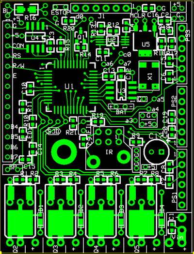
Here's a pic of the top copper layer and silkscreen. Keep in mind that the entire board is only 2.5" (63.5mm) tall.
Some of the patterns look a little "funny" because they are laid out to accept more than one package style. For example, Q's 2-5 can accept MOSFET's in either DPAK, or TO-220 (stood up)
Thanks for all the suggestions. I'm gonna go with the "triple check" method and hope for the best!
steve


Bookmarks