Any tips for 4-layer boards?


Closed Thread
Results 1 to 31 of 31

Hybrid View

  1. #1
    Join Date
    Nov 2003
    Location
    Greece
    Posts
    4,132


    Did you find this post helpful? Yes | No

    Default

    Triple check. What else can I suggest?

    What is your design program? In Eagle there are some tools that help to find shorts or unconnected parts.

    Use these tools to make it easier for checking.

    Photos would be great for this!

    Good luck and keep us posted.

    Ioannis

  2. #2
    Join Date
    Jan 2009
    Location
    California, USA
    Posts
    323


    Did you find this post helpful? Yes | No

    Default

    Thanks Guys for all the good suggestions!

    If this thing works well I hope to make a commercial product out of it, so ease of assembly and a minimum amount of "external" wiring that needs to be hand soldered is important.
    I want 6 boards to build prototypes, and if all goes well I'll order 100 more for my second round. So it's not just a "one of" project. and It needs to be easy to assemble and reasonably "proffesional".

    In the long run, I think that Ioannis had the most practical suggestion for this board.... Triple Check!! (I knew that anyway)

    I don't think that a pair of stacked 2 layer boards saves any money on board costs (4-layer costs less than twice as much as 2 layer), but probably does add quite a bit to assembly time.

    I already tried putting some parts on the backside of the board, but that didn't seem to help. The back is already dense with traces and parts on the back just eats up space where traces need to go and nothing is really gained. Besides, I dislike populating both sides on SMD boards because it's a bitch to keep parts from falling off the bottom when the board is in the oven and I don't relish the idea of soldering one side by hand. I know there's special glues available for that, but that takes more time so I'd rather not populate both sides if I can avoid it.
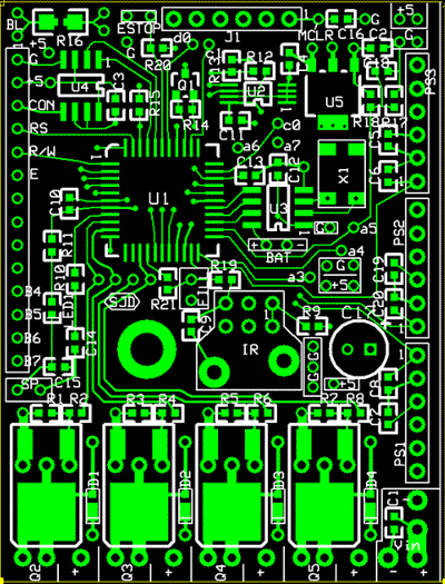
    I'm not a big fan of jumpers and "air wires". I DO use them sometimes, but again, it means more hand soldering and possibility of problems. And I'm afraid I'd need many of them for this board. Besides, jumpers require through holes, which kills space on BOTH sides of a board.

    I think I'm doomed to go with 4-layer boards on this one. It's OK. I need to learn to become proficient at 4-layer anyway since parts keep getting smaller and smaller, and 4-layer does have some advantages with noise immunity.

    I use DIPTrace for my schematic layout, and if I want quite a few boards I use DIPTrace for the board layout also. However, if I just need a few small boards at the lowest possible cost, then I order them from ExpressPCB, which means I'm stuck using their irritating board layout software. (Love their board quality and prices, hate the layout software)

    DIPTrace does have some good tools for verifying the integrity of networks and the like. And it IS possible (with a little work) to import the netlist from DIPTrace to ExpressPCB, so I'm pretty sure my board layout matches the schematic OK.

    I tried Eagle for a few boards, but I just didn't like it much. It seemed difficult and non-intuitive to learn and I finally gave it up. DIPTrace is more compatible with my brain I think.

    I worked on the board a bunch last night and I think I'm about done. I need to double check the footprints of a few items one more time, and also change the pad sizes where the LCD connects, but I think it's about ready to submit... I hope.

    Here's a pic of the top copper layer and silkscreen. Keep in mind that the entire board is only 2.5" (63.5mm) tall.


    Some of the patterns look a little "funny" because they are laid out to accept more than one package style. For example, Q's 2-5 can accept MOSFET's in either DPAK, or TO-220 (stood up)

    Thanks for all the suggestions. I'm gonna go with the "triple check" method and hope for the best!


    steve

  3. #3
    Join Date
    Jul 2003
    Posts
    2,358


    Did you find this post helpful? Yes | No

    Default

    If you want to make a commercial product, bear in mind that a THOUSAND VIAS will still cost less than a four layer board (which is basically two two-layer boards glued together). The only reason I can ever think of going into multi-layers is either Screening or Power Dissipation purposes. With good CAD software (and a good PCB manufacturer) your track separation can be as little as 0.15mm and there should be no need for four layers.

    (For those who don't know, a VIA is a tiny plated hole connecting two layers of a board.)

  4. #4
    Join Date
    Nov 2003
    Location
    Greece
    Posts
    4,132


    Did you find this post helpful? Yes | No

    Default

    I have not any experience wit 4 layers so cannot say if they are more expensive that many vias or not. But if Melanie says so, I accept it as a fact.

    So, indeed it looks dense enough but may be if you select other PIC pins thing can get easier.

    For your checking, does your software have any tools? Like highlighting the electric connections or showing the shorts, etc?

    Ioannis

  5. #5
    Join Date
    Jan 2009
    Location
    Miami, Florida USA
    Posts
    699


    Did you find this post helpful? Yes | No

    Default

    Hi,

    I have done many 2-layer SMD designs, but I have never done a 4-layer design. I agree with Melanie that the preferred way to go is to use many vias with 2-layer boards. There are many useful design tips in the next PDF document.

    http://www.alternatezone.com/electro...torialRevA.pdf

    I use pad2pad instead of expressPCB. Their software is very user friendly and it has features to check your design for flaws.

    Also, there are ways for programing your chip on board without having to solder a connector for programming purposes. Well, keep us posted about your project.

    Robert

  6. #6
    Join Date
    Oct 2005
    Location
    Loveland CO USA
    Posts
    83


    Did you find this post helpful? Yes | No

    Default

    Steve,

    Will U5 get hot? I usually use a larger pad as a heat sink.
    Is there much power lost in Q2,3,4,5? I usually have a large collector pad on all layers. This works as a heat sink and carries the heat to the other side of the board.

    U3,C12 spacing?

    Often a LCD display needs a “pot” to set contrast.

    Mounting holes?

    When I do 4 layer boards I usually use one of the inter layers as ground.
    The other inter layer may have large areas of +5, +3.3 and a hand full of hard to rout traces. I usually have signal traces on the outside.

    If there are noise issues, I may have the outside layers as ground and power planes. This sandwiches the signal traces between planes of copper. (FCC issues)

    Using ball-grid arrays I need two signal layers, power, ground, and two more signal layers.

    ron

  7. #7
    Join Date
    Jan 2009
    Location
    California, USA
    Posts
    323


    Did you find this post helpful? Yes | No

    Default Gonna try harder

    Thanks to everyone for all the good advice!
    I'd hoped to get my board design submitted last week, but I think I need to sit on it and think for a while longer first.
    I've got other obligations this week and may not get to work on it for a few days now.


    Melanie,
    Using more vias instead of more layers sounds great! But I just couldn't get there.... I ended up with too many traces on the backside and carved up my ground plane and had problems with islanding and I *still* couldn't quite get it all to fit.
    With 4 layers I can run traces on both outer layers with power and ground internal and it gets LOTS easier for this poor old boy...
    I'm sure the problem is all about my lack of skill. I haven't done all that much board design and I've usually got plenty real estate to work with.


    Ioannis,
    Yes, I think I need to shuffle a few pins around. But some are pretty much fixed by function (many of the sensors need an ADC pin), and some pins are fixed by... habit (I use the same pins for the LCD on several projects so it's easier to remember what's what.)
    Part of the problem is that the "core" of the circuit was stolen from a previous project, so the layout on that chunk might not be ideal for this project.

    Anyway, I'm going to toss all the parts down on the board again and start over and see if I can cram it onto two layers.


    Robert,
    Thanks for the link to the PCB Design Tutorial. That was a worthy read and may provide some useful tips for me. Much appreciated!
    Yeah, I know I can ditch the programming connector. I eliminated it on the 2 layer design (still couldn't make it all fit), but there was enough space after going to 4-layer that I snuck it back in again. If nothing else it brings those PIC pins out where I can use them If I want.


    Ron,

    The power dissipation on the voltage regulator and transistors should be fine. The regulator has already proven itself to not need any more heat sinking (in another project) and the power dissipation on the FET's is low, and the duty cycle is also low. Should be fine.
    I did add an extra set of through holes for those parts so I can use T0-220 parts on a heatsink if I ever need to.

    Yes indeed, got a contrast pot for the LCD. It's digital (U4) so the user can have some control over it without needing to access the board with a screwdriver.
    Got a single big ugly mounting hole right above Q3.

    You use BGA parts? Wow. Way too scary for me still.


    Anyway, I appreciate all of the good advice you folks have given,and later this week I'm going to try and do a better job on layout and see if it'll all cram onto 2 layers.
    You folks have inspired (or shamed) me into trying harder.


    steve

Similar Threads

  1. Labeling Circuit Boards
    By Atom058 in forum General
    Replies: 7
    Last Post: - 1st August 2008, 15:43
  2. making small boards
    By fowardbias in forum Off Topic
    Replies: 4
    Last Post: - 15th April 2008, 08:58
  3. Replies: 8
    Last Post: - 5th January 2007, 05:10

Members who have read this thread : 0

You do not have permission to view the list of names.

Posting Permissions

  • You may not post new threads
  • You may not post replies
  • You may not post attachments
  • You may not edit your posts