AD9850 DDS code


Closed Thread
Results 1 to 16 of 16

Thread: AD9850 DDS code

  1. #1

    Default AD9850 DDS code

    I have bought a cheap DDS module from CHina and want to start by producing a fixed output of 500kHz, there is no LCD or rotary encoder as yet; This is my code:

    include "modedefs.bas"
    pause 1000; allow circuit 1 sec to stabilise
    pulsout porta.0,100;pulse reset pin
    pause 20
    pulsout porta.3,100;Pulse w_clk
    pause 20
    pulsout porta.2,100;pulse fq_ud to set up serial data mode
    pause 20

    shiftout porta.1,porta.3,0,[%10111000];send out tuning word 1 w0-w7
    ;porta.1 is data, porta.3 is W_CLK

    shiftout porta.1,porta.3,0,[%00100100];send out tuning word 2 w8-w15

    shiftout porta.1,porta.3,0,[%01100000];send out tuning word 3 w16-w23

    shiftout porta.1,porta.3,0,[%10000000];send out tuning word 4 w24-w31

    shiftout porta.1,porta.3,0,[%00000000];send out tuning word 5 w32-w39
    pause 10
    pulsout porta.2,100; pulse FQ_UD on data complete, update DDS
    high portb.4
    pause 2000
    low portb.4;flash LED on portb.4 for 2 secs to show data sent
    end

    Needless to say, it wont work. I have also hardwired D0 and D1 to +Vdd and D2 to GND to force serial mode. Any advice?

    John

  2. #2
    Join Date
    Nov 2003
    Location
    Greece
    Posts
    3,806


    Did you find this post helpful? Yes | No

    Default Re: AD9850 DDS code

    Did you remembered to make all port A digital? Normally Port A defaults to Analog or Comparator.

    Ioannis

  3. #3
    Join Date
    Oct 2005
    Location
    Sweden
    Posts
    3,521


    Did you find this post helpful? Yes | No

    Default Re: AD9850 DDS code

    Hi,
    I've only looked briefly at your code but I think your tuning value is wrong.
    For 500kHz you want 500k*2^32/125M = $01 06 24 DD. You're sending $80 60 24 B8 which would equal a frequency way above 60Mhz....

    Try
    Code:
    SHIFTOUT PortA.1, PortA.3, 0, [$DD, $24, $06, $01, $00]
    Also, which PIC are you using? PortA usually contains analog functions which needs to be disabled for the pins to work in digital mode. I don't see that in your code.

    Finaly, when you force serial mode thru the hardware there's no need to do anything else at the startup - atleast I didn't have to. Perhaps your startup code is locking up the AD9850.

    /Henrik.

  4. #4


    Did you find this post helpful? Yes | No

    Default Re: AD9850 DDS code

    Thanks for the replies on the matter.
    Did you remembered to make all port A digital? Normally Port A defaults to Analog or Comparator.
    Im using a 16F628, I thought the SHIFTOUT command automatically made the named ports digital outputs, but will insert a line of code as you suggest.

    I've only looked briefly at your code but I think your tuning value is wrong
    Yes you are right, will change the values and see what happens.

    Finaly, when you force serial mode thru the hardware there's no need to do anything else at the startup
    Thanks for that clarification

  5. #5


    Did you find this post helpful? Yes | No

    Default Re: AD9850 DDS code

    This is the latest code. Gave up on the SEROUT command and tryed the following so that i could slow down the sequence and see LEDs representing the signals. Cannot get anything out of the AD9850 still. I know the DDS module works as I proved it with someone elses software.

    trisb=$0;SET ALL OF PORTB TO OUTPUTS

    RESET VAR PORTB.7
    CLOCK VAR PORTB.6
    DATAPIN VAR PORTB.5
    DONE VAR PORTB.4;DEFINE
    P VAR WORD;WIDTH OF DATA PULSE
    P=50
    Q VAR WORD;PAUSE BETWEEN DATA BITS
    Q=10
    R VAR WORD;PAUSE BETWEEN DATA WORDS
    R=30
    W VAR BYTE;VARIABLE REPRESENTING BYTES 0 TO 5
    W0 VAR BYTE;WORD 0
    W1 VAR BYTE;WORD 1
    W2 VAR BYTE;WORD.2
    W3 VAR BYTE;WORD.3
    W4 VAR BYTE;WORD 5

    ;DATA FOR BINARY WORDS
    W0=$DD;WORD 0 HEX
    W1=$24;WORD 1 HEX
    W2=$06;WORD 2 HEW
    W3=$01;WORD 3 HEX
    W4=$00;WORD 4 HEX

    PORTB=$00; SET ALL PINS LOW
    MAIN:
    PAUSE 2000
    HIGH RESET
    PAUSE P
    LOW RESET; PULSE RESET PIN
    PAUSE R
    W=W0
    GOSUB BYTEOUT

    PAUSE R
    W=W1
    GOSUB BYTEOUT

    PAUSE R
    W=W2
    GOSUB BYTEOUT

    PAUSE R
    W=W3
    GOSUB BYTEOUT

    PAUSE R
    W=W4
    GOSUB BYTEOUT

    PAUSE R
    PULSOUT DONE,3000; ALL 40 BITS SENT

    HIGH RESET; REPEAT SEQUENCE AGAIN
    PAUSE P
    LOW RESET; PULSE RESET PIN
    W=W0
    GOSUB BYTEOUT
    PAUSE R
    W=W1
    GOSUB BYTEOUT
    PAUSE R
    W=W2
    GOSUB BYTEOUT
    PAUSE R
    W=W3
    GOSUB BYTEOUT
    PAUSE R
    W=W4
    GOSUB BYTEOUT
    PAUSE R
    PULSOUT DONE,3000; ALL 40 BITS SENT
    END

    BYTEOUT:;SUBROUTINE TO CLOCK OUT BITS 0 TO 7 OF BINARY WORD W

    PAUSE P
    DATAPIN=W.BIT0
    PAUSE 20
    HIGH CLOCK
    PAUSE P
    LOW CLOCK
    PAUSE 20
    LOW DATAPIN; CLOCK OUT BIT0

    PAUSE Q
    DATAPIN=W.BIT1
    PAUSE 2
    HIGH CLOCK
    PAUSE P
    LOW CLOCK
    PAUSE 2
    LOW DATAPIN; CLOCK OUT BIT1

    PAUSE Q
    DATAPIN=W.BIT2
    PAUSE 2
    HIGH CLOCK
    PAUSE P
    LOW CLOCK
    PAUSE 2
    LOW DATAPIN; CLOCK OUT BIT2

    PAUSE Q
    DATAPIN=W.BIT3
    PAUSE 2
    HIGH CLOCK
    PAUSE P
    LOW CLOCK
    PAUSE 2
    LOW DATAPIN; CLOCK OUT BIT3

    PAUSE Q
    DATAPIN=W.BIT4
    PAUSE 2
    HIGH CLOCK
    PAUSE P
    LOW CLOCK
    PAUSE 2
    LOW DATAPIN; CLOCK OUT BIT4

    PAUSE Q
    DATAPIN=W.BIT5
    PAUSE 2
    HIGH CLOCK
    PAUSE P
    LOW CLOCK
    PAUSE 2
    LOW DATAPIN; CLOCK OUT BIT5

    PAUSE Q
    DATAPIN=W.BIT6
    PAUSE 2
    HIGH CLOCK
    PAUSE P
    LOW CLOCK
    PAUSE 2
    LOW DATAPIN; CLOCK OUT BIT6

    PAUSE Q
    DATAPIN=W.BIT7
    PAUSE 2
    HIGH CLOCK
    PAUSE P
    LOW CLOCK
    PAUSE 2
    LOW DATAPIN; CLOCK OUT BIT7
    PAUSE Q
    RETURN

  6. #6
    Join Date
    Oct 2005
    Location
    Sweden
    Posts
    3,521


    Did you find this post helpful? Yes | No

    Default Re: AD9850 DDS code

    Hi,
    Sorry for the late reply, you've probably figured it out by now.
    But in case you haven't, have you verified that your PIC is actually running?
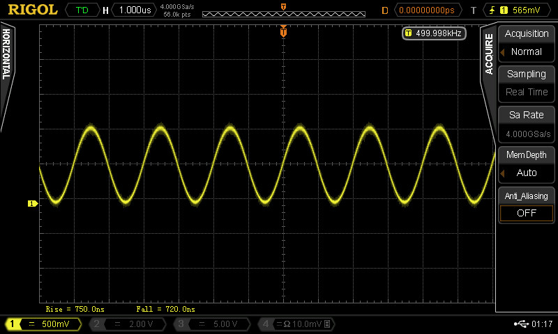
    I've just tried the following code here, all wired up on a breadboard using a 16F628 using a 4MHz x-tal and a AD9850 module, compiled with PBP 3.0.6.4. Module forced into serial mode by tying D0,D1 high and D2 low. It outputs a 500kHz signal as expected:
    Code:
    DEFINE OSC 4
    
    Clk VAR PortB.5                 ' Clock output pin
    Dta VAR PortB.6                 ' Data output pin
    FUd VAR PortB.7                 ' Frequency update output pin
    
    PortB = 0
    TRISB = 0                       ' All outputs
    
    Pause 1000                      ' Let everything power up
    
    ' Tuning word for 500kHz = 500000*2^32/125000000 = 17179869 or, in HEX, $010624DD
    ' The AD9850 wants the least significant byte first:
    SHIFTOUT Dta, Clk, 0, [$DD, $24, $06, $01, $00]
    
    ' Now pulse the Frequency update pin
    FUd = 1 : PauseUS 10 : FUd = 0
    
    ' Blink a LED to show we're alive.
    Done:
      Toggle PortB.3
      Pause 100
    Goto Done
    Here's the result:
    Name:  DSX_20130223011754.jpeg
Views: 5070
Size:  102.8 KB

    /Henrik.

  7. #7
    Join Date
    Oct 2005
    Location
    Sweden
    Posts
    3,521


    Did you find this post helpful? Yes | No

    Default Re: AD9850 DDS code

    Just a follow up to the previous post.
    For reference, here's the "schematic" for the setup I used with the above code. There are a couple of different modules in circulation so make sure the actual signals and not the pin numbers matches your particular module.

    Name:  AD9850-setup.jpg
Views: 8727
Size:  41.7 KB

    If you're programming the PIC in-circuit perhaps the programmer is loading RB6, RB7 (since they are the programming pins) preventing them from operating the AD9850 properly? I'm doing just that with a PICKit3 on my breadboard and don't see any issues but it's a thought.

    /Henrik.

  8. #8


    Did you find this post helpful? Yes | No

    Default Re: AD9850 DDS code

    I now have the circuit working. I dont quite understand why the first attempt didnt work, but the following works for me. Thankyou for taking the time to solve my problem.

    DEFINE OSC 4 ;WE ARE USING A 4MHZ XTAL OSCILLATOR

    CLOCK VAR PortB.6 ;CLOCK SIGNAL IS ON RB6, PIN 12
    DATAPIN VAR PortB.5;DATA SIGNAL IS ON RB5, PIN 11
    FQUD VAR PortB.4 ;FREQUENCY UPDATE ON RB4, PIN 10

    TRISB = 0 ;SET ALL OF PORTB AS OUTPUTS
    PORTB = 0 ;SET ALL OF PORTB LOW

    Pause 1000 ;WAIT FOR CIRCUIT TO STABILISE
    PULSOUT FQUD,10 ;RESET DDS
    SHIFTOUT DATAPIN, CLOCK, 0, [$DD, $24, $06, $01, $00] ;SEND SERIAL DATA TO DDS
    PULSOUT FQUD,10 ;LOAD NEW FREQUENCY 500KHZ

    SHIFTOUT DATAPIN, CLOCK, 0, [$DD, $24, $06, $01, $00] ;SEND SERIAL DATA TO DDS
    PULSOUT FQUD,10 ;LOAD NEW FREQUENCY 500KHZ
    ;SERIAL DATA IS SENT TWICE, IF ONLY SENT ONCE DDS CHIP SOMETIMES LOCKS UP
    END

  9. #9
    Join Date
    Jun 2008
    Location
    Varese , Italy
    Posts
    326


    Did you find this post helpful? Yes | No

    Default Re: AD9850 DDS code

    Hi Henrik,
    I will like to understand what are OUTPUT_1 and OUTPUT_2 : any help? Sine or square ?
    What about the other two outputs ?
    What is the purpose of R_13 Trim ?

    I do not have any schematics for this board nor manual to read ! My board is exactly the one shown in your photo.

    Thanks again for the great help .
    Bye
    Ambrogio
    IW2FVO

  10. #10
    Join Date
    Oct 2005
    Location
    Sweden
    Posts
    3,521


    Did you find this post helpful? Yes | No

    Default Re: AD9850 DDS code

    Hi,
    Not sure, I don't know much about the hardware I'm afraid. I wrote the code and put the board on the shelf.... I'd look at the AD9850 datasheet for details.
    I think both outputs are Sine outputs, the phase relationship between the two outputs is what you set with CONTROL word.

    /Henrik.

  11. #11


    Did you find this post helpful? Yes | No

    Default Re: AD9850 DDS code

    Here's a schematic for the above module

    As I recall the pot will change the duty cycle on the square wave
    and will skew the sine wave


    Name:  Ad9850_ebay.jpg
Views: 7201
Size:  46.2 KB

  12. #12
    Join Date
    Jun 2008
    Location
    Varese , Italy
    Posts
    326


    Did you find this post helpful? Yes | No

    Default Re: AD9850 DDS code

    Henrik and Mark_s,
    thanks for the assistance.
    regards,
    Ambrogio
    IW2FVO

  13. #13
    Join Date
    Aug 2005
    Posts
    42


    Did you find this post helpful? Yes | No

    Default Re: AD9850 DDS code

    Quote Originally Posted by iw2fvo View Post
    I will like to understand what are OUTPUT_1 and OUTPUT_2 : any help? Sine or square ?
    What about the other two outputs ?
    What is the purpose of R_13 Trim ?
    The module has two outputs for Sine Wave and two outputs for Square wave.

    In Henriks handy pin-out picture he shows the two sine waves outputs, the next two pins above are the square wave outputs.

    Played with a module today and the code examples Henrik supplied work great and thank you Henrik.

    The Pic Chips tend to max out at 25khz when pulsing stepper drivers which retricts the speed when running them at say 2000 pulses per revolution. It limits you to a max of around 500 RPM.

    Now with the DDS boards + Pic Chip combination, I had some stepper motors here today hitting over 5000 RPM no problems at all.

    Great little modules and good prices.

    Cheers

    Sean.
    *********************
    http://www.cncdudez.co.uk
    *********************

  14. #14
    Join Date
    Jun 2008
    Location
    Varese , Italy
    Posts
    326


    Did you find this post helpful? Yes | No

    Default Re: AD9850 DDS code

    Sean,
    could I have the circuit diagram for your stepper motor implementation ?
    Thanks
    Ambrogio

  15. #15
    Join Date
    Jun 2008
    Location
    Varese , Italy
    Posts
    326


    Did you find this post helpful? Yes | No

    Default Re: AD9850 DDS code

    Henrik,

    I have used my module today , it is the same model that is shown in your picture.
    I have discovered an intermittent sine wave stream at the two output. This was due to the RESET line that has to be connected to ground.
    This is in my circuit lay_out.
    I hope it will help in some cases.
    Ambrogio

  16. #16
    Join Date
    Oct 2005
    Location
    Sweden
    Posts
    3,521


    Did you find this post helpful? Yes | No

    Default Re: AD9850 DDS code

    Hi,
    Thank you very much for that post!
    I haven't noticed it any of my (two) breadboard sesions with the module. Just measured it and the Reset pin is indeed floating - must have been pure luck it worked for me.

    I wish I could fix the "schematic" but I can't....

    Thanks again!
    /Henrik.

Similar Threads

  1. Calculate tuning value for the AD9850 DDS.
    By HenrikOlsson in forum mel PIC BASIC Pro
    Replies: 16
    Last Post: - 21st July 2018, 00:49
  2. Working code but my layman approach uses too much code space
    By Christopher4187 in forum mel PIC BASIC Pro
    Replies: 4
    Last Post: - 14th December 2012, 20:44
  3. Code: Why is this code greater than 2000 words?
    By DrDreas in forum mel PIC BASIC Pro
    Replies: 9
    Last Post: - 1st June 2007, 19:51
  4. Need help in controlling DDS AD9850/51
    By vu2iia in forum mel PIC BASIC Pro
    Replies: 4
    Last Post: - 7th March 2007, 12:40

Members who have read this thread : 1

You do not have permission to view the list of names.

Posting Permissions

  • You may not post new threads
  • You may not post replies
  • You may not post attachments
  • You may not edit your posts