4 Wire SPI with Shiftin/Shiftout ?


Closed Thread
Results 1 to 19 of 19

Hybrid View

  1. #1
    Join Date
    Feb 2013
    Posts
    1,078

    Default 4 Wire SPI with Shiftin/Shiftout ?

    Hello.
    I'm trying to connect GT21L16S2Y Font ROM IC to PIC16F886.
    I have soldered connections, but have not written code yet, because this chip has separate IN/OUT pins for SPI.

    Below is the draft code which I think should work (have not tried it yet).

    Code:
    SCLK	VAR	PORTB.5 'CLOCK
    TC	VAR	PORTC.0 'TO CHIP - WRITE
    FC	VAR	PORTC.6 'FROM CHIP - READ
    RST	VAR	PORTB.4 'RESET
    I VAR BYTE 'COUNTER VAR
    X VAR BYTE 'TEMP VAR
    FONT VAR BYTE [8] 'FONT ARRAY


    Reader: 'Font reading outline
    LOW RST         ' Ready for transfer
       Shiftout TC, SCLK, 5, [$03,$0] ' Send write command, set start offset 
    For I=0 to 7 'read 8 bytes of data
       Shiftin FC, SCLK, 5, [x]
    FONT[I]=X 'WRITE TO ARRAY
    next
    HIGH RST        ' Reset IC
    Return
    And here is screenshot from the datasheet. It is in chinese, but diagrams show things clearly.

    So I'm on the proper way or not?

    Name:  GTL.jpg
Views: 483
Size:  419.7 KB

  2. #2
    Join Date
    Oct 2005
    Location
    Sweden
    Posts
    3,521


    Did you find this post helpful? Yes | No

    Default Re: 4 Wire SPI with Shiftin/Shiftout ?

    I have soldered connections, but have not written code yet, because this chip has separate IN/OUT pins for SPI.
    Of course they have separate in/out pins, that's how SPI works.

    So I'm on the proper way or not?
    I think so. But for starters, looking at the image you posted you should send an 8 bit command followed by a 24 bit address (32bits in total), you're only sending 16.

  3. #3
    Join Date
    Feb 2013
    Posts
    1,078


    Did you find this post helpful? Yes | No

    Default Re: 4 Wire SPI with Shiftin/Shiftout ?

    Well, MAX7219, DS1302 we use only 3 pins.
    Yes, I'm missing two more bytes there, will add them later and post back

  4. #4
    Join Date
    Oct 2005
    Location
    Sweden
    Posts
    3,521


    Did you find this post helpful? Yes | No

    Default Re: 4 Wire SPI with Shiftin/Shiftout ?

    The MAX7219 is not capable of outputting any data, therefor no data out pin.
    DS1302 might work with SHIFTIN/SHIFTOUT but its interface isn't really SPI.

  5. #5
    Join Date
    May 2013
    Location
    australia
    Posts
    2,389


    Did you find this post helpful? Yes | No

    Default Re: 4 Wire SPI with Shiftin/Shiftout ?

    So I'm on the proper way or not?
    not. the shiftout shiftin commands leave the clock line high on completion{mode 5} so when you swap between them the slave device will see
    a false rising edge and you lose a data bit .

    nearly all respectable pic16/18 chips have a mssp module why not just use it ?
    or write a bit banger to suit

    Well, MAX7219, DS1302 we use only 3 pins
    which are not spi anyway , its a stupid argument
    Warning I'm not a teacher

  6. #6
    Join Date
    Feb 2013
    Posts
    1,078


    Did you find this post helpful? Yes | No

    Default Re: 4 Wire SPI with Shiftin/Shiftout ?

    Yes, I tried with mode 5 and it does not works, it also does not works with mode 4 or others.
    MSSP or whatever it is, might be good, but are there direct support statements in PBP ?
    And also, I already have pre-wired devices and they're meant to be in that way.

    The code below does not works - it returns all 255.

    Code:
    ;----[16F886 Hardware Configuration]--------------------------------------------
    #CONFIG
    cfg1 = _INTRC_OSC_NOCLKOUT    ; INTOSCIO oscillator: I/O function on RA6/OSC2/CLKOUT pin, I/O function on RA7/OSC1/CLKIN
    cfg1&= _WDT_ON                ; WDT enabled
    cfg1&= _PWRTE_OFF             ; PWRT disabled
    cfg1&= _MCLRE_OFF             ; RE3/MCLR pin function is digital input, MCLR internally tied to VDD
    cfg1&= _CP_OFF                ; Program memory code protection is disabled
    cfg1&= _CPD_OFF               ; Data memory code protection is disabled
    cfg1&= _BOR_OFF               ; BOR disabled
    cfg1&= _IESO_ON               ; Internal/External Switchover mode is enabled
    cfg1&= _FCMEN_ON              ; Fail-Safe Clock Monitor is enabled
    cfg1&= _LVP_OFF               ; RB3 pin has digital I/O, HV on MCLR must be used for programming
    cfg1&= _DEBUG_OFF             ; In-Circuit Debugger disabled, RB6/ICSPCLK and RB7/ICSPDAT are general purpose I/O pins
      __CONFIG _CONFIG1, cfg1
    
    
    cfg2 = _BOR40V                ; Brown-out Reset set to 4.0V
    cfg2&= _WRT_OFF               ; Write protection off
      __CONFIG _CONFIG2, cfg2
    
    
    #ENDCONFIG


    'chip configs
    TRISA=%01000000  'SET A TO OUTPUT   1=input
    TRISC=%00000000   'set half C for in/out
    TRISB=%00000000   'set PortB to output
    ANSELH=%00000000   ' ADC OFF B
    ANSEL=%000000000 'configure PortA as digital except first 2
    ADCON1=%10000000  'adc justify
    OSCCON=%01110101  'SET FREQUENCY TO 8MHZ
    WPUB=%00000000    'turn off Pullups
    CM1CON0=0         'DISABLE COMPARATORS
    CM2CON0=0         'SAME HERE
    
    
    DEFINE OSC 8   
    DEFINE ADC_BITS 10
    DEFINE ADC_CLOCK 3
    DEFINE ADC_SAMPLEUS 50
    'lcd config
    pause 10
    ' Set LCD Data port 
    DEFINE LCD_DREG PORTC  
    DEFINE LCD_DBIT 4  
    DEFINE LCD_RSREG PORTB  
    DEFINE LCD_RSBIT 0  
    DEFINE LCD_EREG PORTB  
    DEFINE LCD_EBIT 1  
    DEFINE LCD_BITS 4  
    DEFINE LCD_LINES 2  
    DEFINE LCD_COMMANDUS 1500  
    DEFINE LCD_DATAUS 44


    SCLK	VAR	PORTB.5 'CLOCK
    TC	VAR	PORTC.0 'TO CHIP - WRITE
    FC	VAR	PORTC.6 'FROM CHIP - READ
    RST	VAR	PORTB.4 'RESET
    I VAR BYTE 'COUNTER VAR
    X VAR BYTE 'TEMP VAR
    FONT VAR BYTE [8] 'FONT ARRAY
    
    
    Reader: 'Font reading outline
    LOW RST         ' Ready for transfer
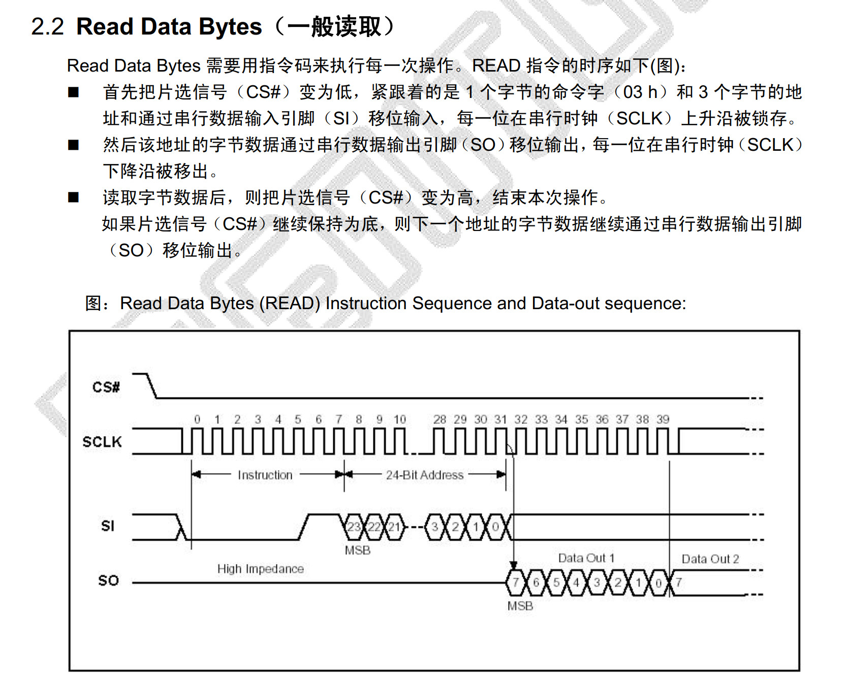
       Shiftout TC, SCLK, 5, [$03,$100,$00,$0] ' Send write command, set start offset 
    For I=0 to 255 'read 8 bytes of data
       Shiftin FC, SCLK, 5, [x]
    LCDOUT $fE, $C0, DEC I,32, DEC X
    Pause 200
    next
    HIGH RST        ' Reset IC
    GOTO READER

  7. #7
    Join Date
    Oct 2005
    Location
    Sweden
    Posts
    3,521


    Did you find this post helpful? Yes | No

    Default Re: 4 Wire SPI with Shiftin/Shiftout ?

    I'd try mode 5 for SHIFTOUT and mode 6 for SHIFTIN.
    I would also add some code to make sure #CS is high for a while during startup. Then I would add a scope or logic analyzer to verify that what you think is happening is actually happening at the hardware level.

Similar Threads

  1. porta problems during shiftout/shiftin
    By eccessivo in forum Serial
    Replies: 2
    Last Post: - 19th July 2013, 19:00
  2. Shiftout - shiftin question
    By Lasse1 in forum mel PIC BASIC Pro
    Replies: 8
    Last Post: - 5th April 2010, 16:34
  3. 16f877A and shiftin shiftout
    By ghdsfier8 in forum mel PIC BASIC Pro
    Replies: 3
    Last Post: - 22nd February 2008, 13:47
  4. shiftout and shiftin
    By Ron Marcus in forum mel PIC BASIC Pro
    Replies: 1
    Last Post: - 24th April 2006, 15:01
  5. Shiftin/Shiftout
    By paul.mcallister in forum mel PIC BASIC Pro
    Replies: 1
    Last Post: - 11th May 2005, 04:24

Members who have read this thread : 3

You do not have permission to view the list of names.

Posting Permissions

  • You may not post new threads
  • You may not post replies
  • You may not post attachments
  • You may not edit your posts